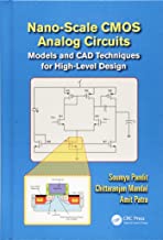
Nano-Scale CMOS Analog Circuits: Models & CAD Techniques for High-Level Design
Original price was: ₹15,078.00.₹12,062.40Current price is: ₹12,062.40.
ISBN: 9781466564268
Author/Editor: Soumya Pandit
Publisher: CRC Press
Year: 2014
1 in stock (can be backordered)
Description
Reliability concerns and the limitations of process technology can sometimes restrict the innovation process involved in designing nano-scale analog circuits. The success of nano-scale analog circuit design requires repeat experimentation, correct analysis of the device physics, process technology, and adequate use of the knowledge database.
Starting with the basics, Nano-Scale CMOS Analog Circuits: Models and CAD Techniques for High-Level Design introduces the essential fundamental concepts for designing analog circuits with optimal performances. This book explains the links between the physics and technology of scaled MOS transistors and the design and simulation of nano-scale analog circuits. It also explores the development of structured computer-aided design (CAD) techniques for architecture-level and circuit-level design of analog circuits.
The book outlines the general trends of technology scaling with respect to device geometry, process parameters, and supply voltage. It describes models and optimization techniques, as well as the compact modeling of scaled MOS transistors for VLSI circuit simulation.
?Includes two learning-based methods: the artificial neural network (ANN) and the least-squares support vector machine (LS-SVM) method
?Provides case studies demonstrating the practical use of these two methods
?Explores circuit sizing and specification translation tasks
?Introduces the particle swarm optimization technique and provides examples of sizing analog circuits
?Discusses the advanced effects of scaled MOS transistors like narrow width effects, and vertical and lateral channel engineering
Nano-Scale CMOS Analog Circuits: Models and CAD Techniques for High-Level Design describes the models and CAD techniques, explores the physics of MOS transistors, and considers the design challenges involving statistical variations of process technology parameters and reliability constraints related to circuit design.
Additional information
| Weight | 0.703 kg |
|---|
Product Properties
| Year of Publication | 2014 |
|---|---|
| Table of Contents | Introduction Introduction Characterization of Technology Scaling Analog Design Challenges in Scaled CMOS Technology Motivation for CAD Techniques Conventional Design Techniques for Analog IC Design Knowledge-based CAD Technique for Analog ICs Summary and Conclusion High-Level Modeling and Design Techniques Introduction High-Level Model Behavioral Model Generation Technique Introduction to Optimization Techniques Some Important Optimization Algorithms Multi-Objective Optimization Method Pareto Optimal Front Design Space Exploration Computational Complexity of a CAD Algorithm Technology aware Computer Aided IC Design Technique Commercial Design Tools Modeling of Scaled MOS Transistor for VLSI Circuit Simulation Introduction Device Modeling Compact Models Long-Channel MOS Transistor Threshold Voltage Model for Long-channel Transistor with Uniform Doping SPICE Level Drain Current Model SPICE Level I-V Model MOSFET Capacitances Short-Channel MOS Transistor Threshold Voltage for Short-Channel MOS Transistor I-V Model for Short-Channel MOS transistor Weak Inversion Characteristics of a Scaled MOS transistor Hot Carrier Effect Source-Drain Resistance Model Compact Modeling Salicide Technology Physical Model for Output Resistance Poly-silicon Gate Depletion Effect Effective Channel Length and Width Summary and Conclusion Performance and Feasibility Model Generation using Learning based Approach Introduction Requirement of Leaning-based Approaches Regression Problem for Performance Model Generation Some Related Works Preliminaries on Artificial Neural Network Neural Network Model Development Case Study 1: Performance Modeling of CMOS Inverter Case Study 2: Performance Modeling of Spiral Inductor Dynamic Adaptive Sampling Introduction to Least Squares Support Vector Machines Feasible Design Space and Feasibility Model Case Study 3: Combined Feasibility and Performance Modeling of Two-Stage Operational Amplifier Case Study 4: Architecture-Level Performance Modeling of Analog Systems Meet-in-the-Middle Approach for Construction of Architecture-Level Feasible Design Space Case Study 5: Construction of FeasibilityModel at Architecturelevel of an Interface Electronics for MEMS Capacitive Accelerometer System Summary and Conclusion Circuit Sizing and Specification Translation Introduction Circuit Sizing as a Design Space Exploration Problem Particle Swarm Optimization Algorithm (PSO) Case Study 1: Design of a Two Stage Miller OTA Case Study 2: Synthesis of On-chip Spiral Inductors Case Study 3: Design of a nano-scale CMOS inverter for Symmetric Switching Characteristics The gm/ID Methodology for Low Power Design High-Level Specification Translation Summary and Conclusion Advanced Effects of Scaled MOS Transistors Introduction Narrow Width Effect on Threshold Voltage Channel Engineering of MOS Transistor Gate Leakage Current High- Dielectrics and Metal-Gate/High- CMOS Technology Advanced Device Structures of MOS Transistors Noise Characterization of MOS Transistors Gate Resistance and Substrate Network Model of MOS Transistor for RF Applications Summary and Conclusion Process Variability and Reliability of Nano-scale CMOS Analog Circuits Introduction Basic Concepts on Yield and Reliability Sources of Variations in Nanometer Scale Technology Systematic Process Variations Random Process Variations Statistical Modeling Physical Phenomena Affecting the Reliability of Scaled MOS Transistor Physical Model for MOSFET Degradation due to HCI Reaction-Diffusion Model for NBTI Reliability Simulation for Analog Circuits Summary and Conclusion Bibliography |
| Author | Soumya Pandit |
| ISBN/ISSN | 9781466564268 |
| Binding | Hardback |
| Edition | 1 |
| Publisher | CRC Press |
You must be logged in to post a review.


Reviews
There are no reviews yet.